
aPlanner for Wafer Fabrication
Navigate technology transitions with predictive planning intelligence built for semiconductor complexity.
Target figures are design targets from simulation on synthetic fab data. aPlanner has no customer deployments yet; first pilot results are expected in 2027.
Semiconductor Foundry Market
Wafer fabrication demands planning tools built for semiconductor-grade complexity
Semiconductor fabrication involves hundreds of process steps, multi-billion dollar capital investments, and technology transitions that redefine capacity every few years. Traditional planning tools were never designed for this level of complexity.
How aPlanner addresses wafer fab challenges
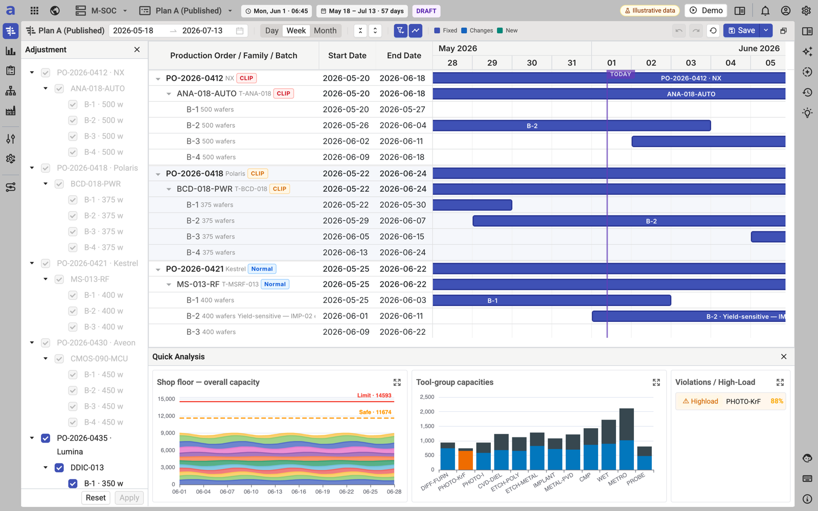
Purpose-built for semiconductor manufacturing, aPlanner brings node-aware intelligence to every planning decision — from capacity allocation to yield-integrated scheduling.
Node-aware capacity planning
Model capacity by technology node, with automatic reallocation as products migrate between nodes. Simulate node transitions with yield learning curves built into the model.
WIP optimization
Balance WIP levels across the fab to maximize throughput while minimizing cycle time variability. aPlanner identifies bottlenecks and recommends WIP targets by operation.
Equipment utilization optimization
Scheduling that maximizes utilization of critical tools while respecting maintenance windows, qualification requirements, and priority orders.
Yield ramp modeling
Incorporate yield learning curves into planning, with scenario analysis for optimistic and pessimistic ramp assumptions. Plan for actual output at each stage of the yield journey.
Estimated opportunity for wafer fabrication
Design targets derived from published industry benchmarks and simulation on synthetic data. aPlanner has no deployments in this segment yet.
| Value Driver | Target impact | Estimated annual value (Large Fab) |
|---|---|---|
| Capacity Utilization | +5-10% | $50-100M |
| WIP Reduction | -15-25% | $10-20M |
| Cycle Time Improvement | -10-20% | $20-40M |
| Planning Efficiency | -70% time | $2-4M |
Target figures are design targets from simulation on synthetic fab data. aPlanner has no customer deployments yet; first pilot results are expected in 2027.
Ready to optimize your wafer fab planning?
See how aPlanner can deliver node-aware capacity planning, WIP optimization, and yield-integrated scheduling for your semiconductor fabrication operations.