
aPlanner for NAND Flash — built for Korean fabs
Yield-aware, scenario-driven AI planning for multi-step wafer processes: wafer starts, good die and bin mix planned together; node migrations planned as one system; every re-plan explained.
Pre-commercial MVP validated on synthetic NAND-flash datasets. First Korean fab pilot planned for 2027.
Target figures are design targets from simulation on synthetic fab data. aPlanner has no customer deployments yet; first pilot results are expected in 2027.
Korea: the center of gravity of memory
No customer or pilot is signed. Sources: U.S. ITA market brief, KOTRA / Invest Korea (2026).
NAND Flash presents unique planning challenges that generic tools cannot address
NAND Flash memory manufacturing is among the most complex planning environments in the world. Long cycle times, extreme yield variability, continuous technology transitions, and volatile demand create challenges that spreadsheets and legacy planning tools simply cannot handle.
How aPlanner addresses NAND Flash challenges
Every capability is designed for memory production — from bit-level forecasting to yield-aware scheduling. The same engine, data model and screens apply unchanged from the demo foundry to a 300-layer NAND fab.
Yield-aware constraint scheduling
The optimizer takes live yield and bin distributions per process step as inputs, so wafer starts, expected good die and bin mix are planned together across 50–100+ steps — instead of scheduling starts and hoping the yield follows.
Node-migration planning
Models learning curves, ramp rates and capacity shifts when a line moves 176L → 236L → 300L+, planning old and new nodes as one system with shared tools and demand.
Explainable re-planning
Every schedule change carries the triggering event, the constraints it hit and the KPI delta; frozen / flex / far zones bound how much the plan may move; the planner approves, edits or rejects in Korean or English.
Bit-level forecasting by density tier
Forecast and plan at the bit-density level (128Gb, 256Gb, 512Gb, 1Tb) with automatic roll-up to die and wafer levels. Ensemble models per tier with confidence intervals; demand sensing for hyperscaler swings.
Yield-aware constraint scheduling
Live yield and bin distributions per process step are inputs to the optimizer, so wafer starts, expected good die and bin mix are planned together. Plan for actual output — not theoretical capacity.
Node-migration planning
Model the ramp of a new generation (236L, 300L+) alongside legacy production — learning curves, capacity shifts and shared tools in one planning model, so commitments survive the transition.
Global capacity balancing
Balance production across fabs worldwide, considering regional demand, shipping times, and fab-specific capabilities. aPlanner optimizes the global network, not just individual sites.
Strategic inventory optimization
Optimize die inventory levels across the network. Balance responsiveness against working capital. aPlanner recommends optimal die bank positions by product family and geography.
Multi-month horizon planning
Make wafer start decisions months in advance with uncertainty modeling. aPlanner simulates demand scenarios and yield outcomes to recommend start quantities that maximize upside and minimize risk.
Estimated opportunity for a large NAND fab
The problem analysis is strong; the gains are design targets. The columns below show the industry baseline, the target aPlanner is built against, and the estimated annual value at stake — not results.
| Value driver | Industry baseline | aPlanner design target | Estimated annual value at stake |
|---|---|---|---|
| Forecast accuracy | 55–65% | Target 85–90% | US$20–40M |
| Planning cycle time | 3–5 days | Target < 30 min full-fab schedule | US$5–10M |
| Inventory | Baseline | Target −15–25% | US$30–50M working capital |
| On-time delivery | 85–90% | Target 95–99% | US$10–20M |
| Expediting costs | Baseline | Target −40–60% | US$5–15M |
Estimated opportunity from published industry benchmarks and simulation on synthetic NAND-flash datasets; the entry investment is KRW 125–250M for assessment plus pilot, then KRW 120–300M per year for Starter. aPlanner has no customer deployments; pilot results are expected in 2027.
Yield excursion: contain and replan in minutes
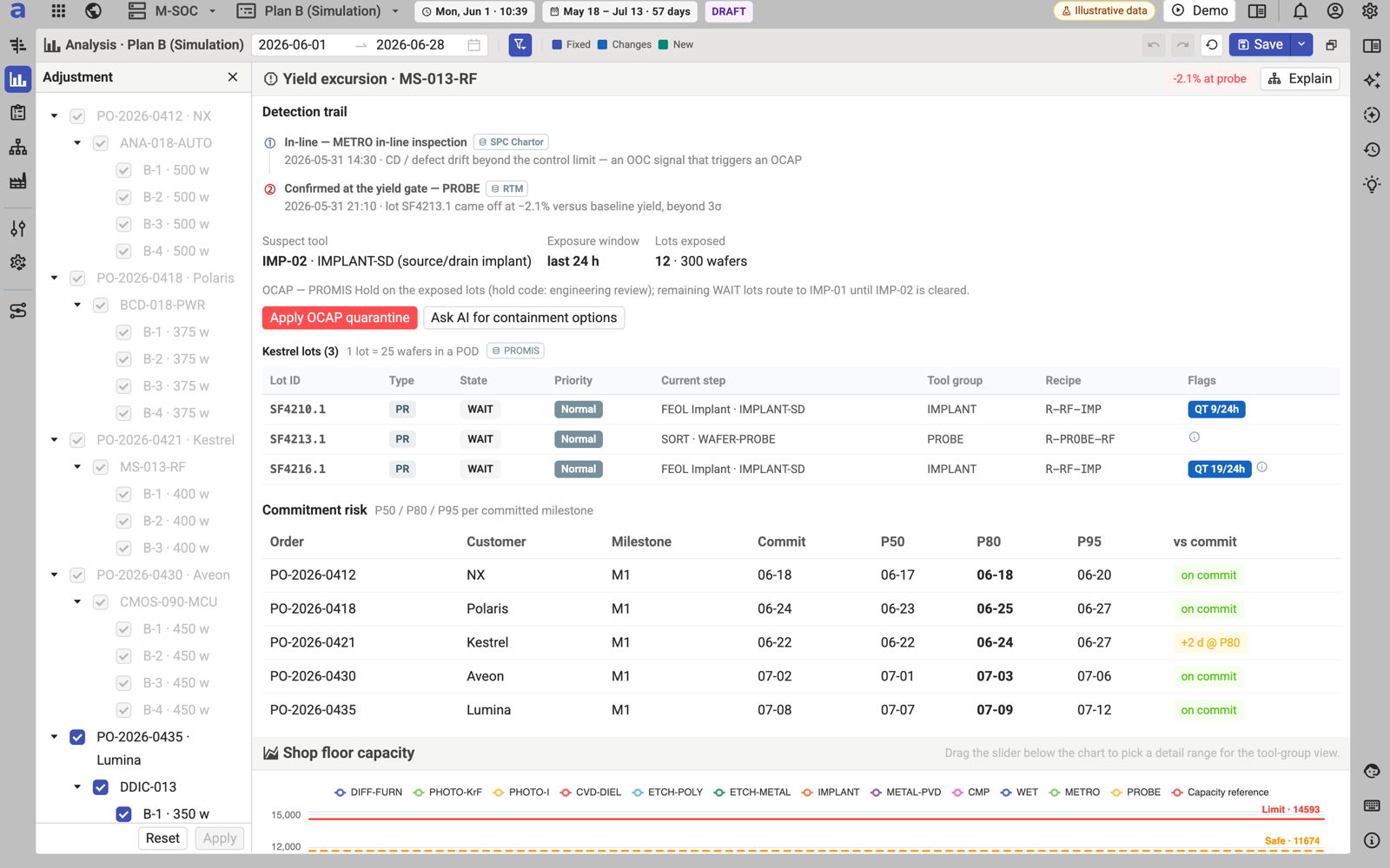
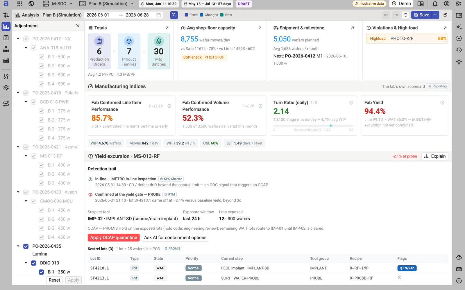
In a NAND fab, probe confirms yield six to eight weeks after start. When metrology flags a drift and probe confirms −2.1%, the engine shows the affected lots, the suspect tool and the commitment exposure at P50 / P80 / P95, proposes an OCAP quarantine and two re-plan scenarios — and the wafer-start correction that keeps the good-die commitment.
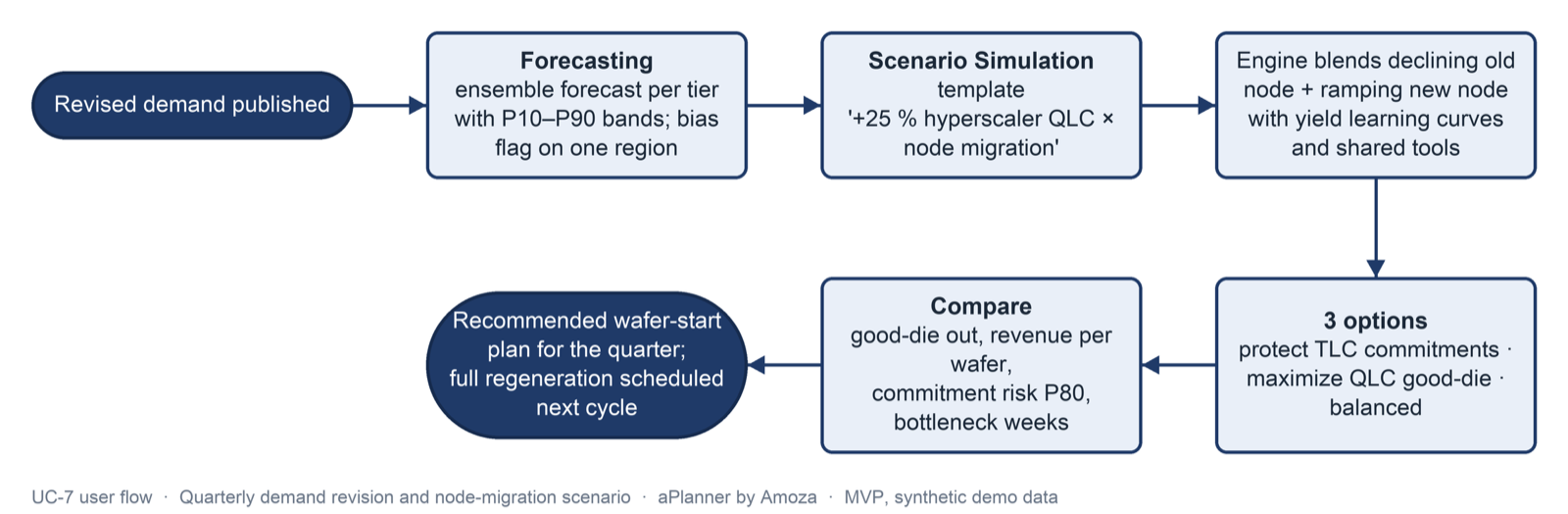
Hyperscaler pull-in? The engine proposes which TLC starts to defer and shows the revenue-per-wafer effect of the bin mix.
All eight use cases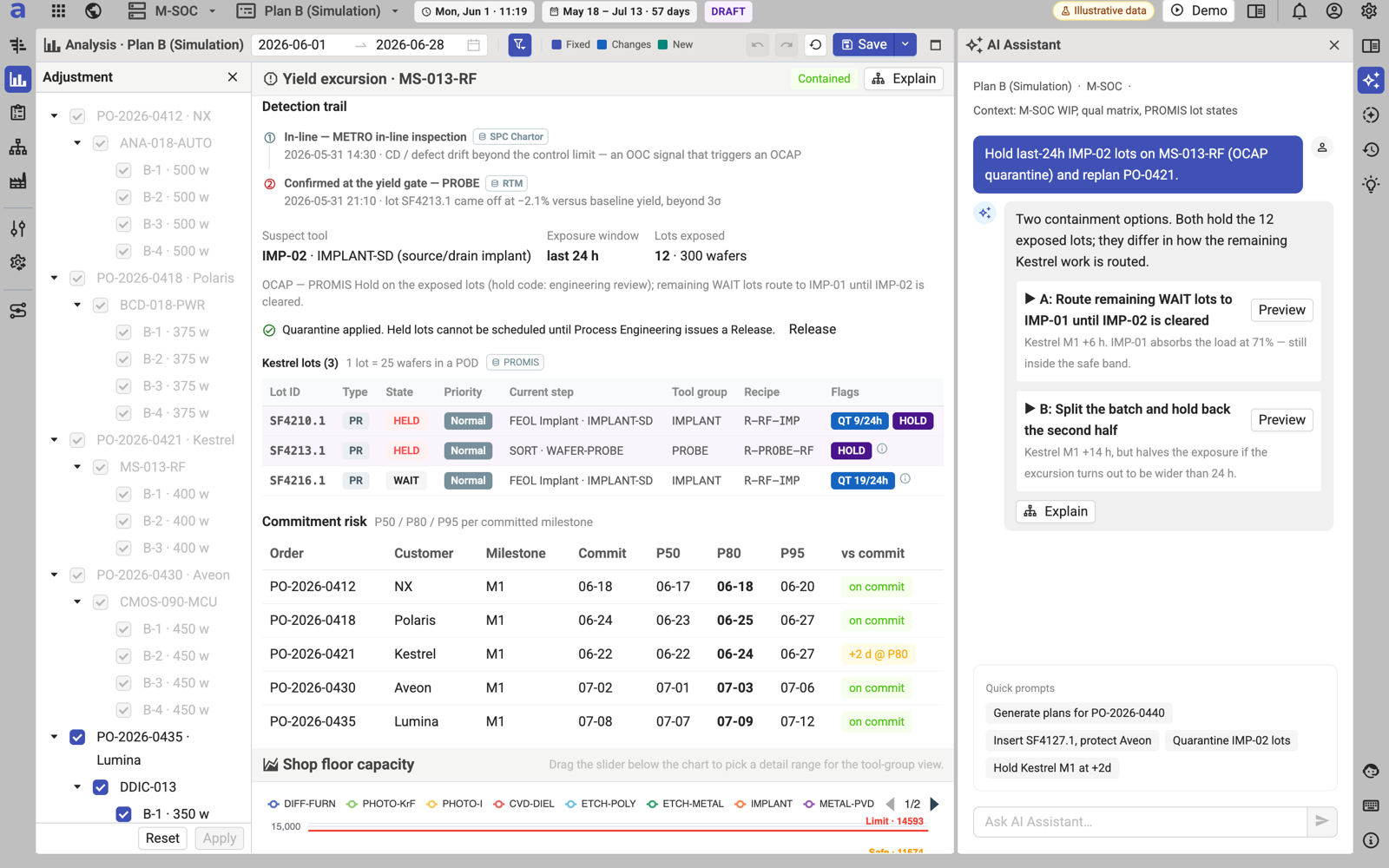
Three advantages no overseas vendor can copy quickly
Overseas vendors fail the Korean fab’s first three questions: where is my data, does it talk to my MES, and who answers the phone in Korean at 7 a.m.? aPlanner answers all three.
Data stays in the fab
On-premise or private cloud inside the fab network — air-gapped option, read-only connectors first, no production data leaves the site; K-ISMS / ISO 27001 roadmap.
Korean fabs reject off-site production data. Cloud-first SAP IBP, o9 and Kinaxis stall in the security review; aPlanner clears the #1 objection on day one.
Korean systems landscape
Pre-built connectors for in-house MES, SAP ERP, yield / bin databases and planner spreadsheets; Korean SI / MES partners deliver; two Siemens Industry Software architects advise on MES / PLM integration.
Incumbents need 12–18 months of system-integrator customization; aPlanner targets 8–12 weeks to a running pilot because the Korean stack is the default, not a project.
Korean users, Korean support
Korean UI, reports and approval workflow; Korean hires in 2027 (planning domain, MES integration, business development); founder and support within an hour of the Yongin–Pyeongtaek cluster; KRW contracts with a Korean company.
Overseas vendors support in English from another time zone; aPlanner sits next to the planner, in Korean, at roughly half the incumbents’ entry price (Starter KRW 120–300M).
aPlanner for Korean fabs — the specifics
Yongin–Pyeongtaek cluster
Every new fab in the cluster will need a planning team. The founder is based in Suwon; Amoza Korea will sit in Incheon Songdo or Suwon — within an hour of the fabs.
On-prem deployment
On-premise or private cloud inside the fab network, air-gapped option, read-only connectors first. K-ISMS / ISO 27001 roadmap.
Korean MES / SAP connectors
Pre-built connectors for in-house MES, SAP ERP, yield / bin databases and planner spreadsheets; Korean SI / MES partners deliver; Siemens Industry Software advisors on MES / PLM integration.
Korean UI & support
Korean UI, reports and approval workflow; support from the Korea office in Korean; Korean hires in 2027 (planning domain, MES integration, business development).
Funding levers for customers
K-Chips Act investment credits and the national AI-manufacturing agenda ("AI factory" programs) can co-fund planning modernization; we map the options during the readiness assessment.
KRW pricing, pilot first
Planning Readiness Assessment KRW 50–100M (2–4 weeks) → pilot on one line KRW 75–150M (8–12 weeks) → Starter KRW 120–300M/yr.
Be the first Korean memory fab to pilot aPlanner
A paid planning readiness assessment on one fab or line, then an 8–12-week pilot inside your network with your planners. 2027 slots are limited to two or three design partners.